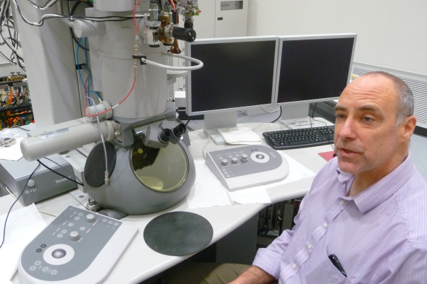
Ames Lab’s Matt Kramer with the Tecnai transmission electron microscope at the new Sensitive Instrument Facility (SIF). The microscope was moved to the SIF from Wilhelm Hall on the Iowa State University campus.
In 2015 Ames Laboratory scientists who investigate materials’ fundamental properties received their Christmas presents early.
In November and December technicians unpacked and installed around $6 million worth of high-tech microscopes, some capable of identifying individual atoms and how they’re arranged in materials. The three new devices joined one already owned by the lab, a Department of Energy (DOE) facility Iowa State University manages on its campus.
The equipment is installed at the lab’s Sensitive Instrument Facility (SIF), a fortress against interference recently finished northwest of the ISU campus. In my last post, I described the many steps the building’s designers took to keep vibrations and electromagnetic noise from disturbing the powerful microscopes inside.
In this post I’ll tell you more about the devices themselves. With their power, scientists can better understand materials and develop new ones that save energy and improve the performance of devices we use every day.
Ames Lab’s specialty in materials science dates back to its roots in the Manhattan Project to build the first atomic bomb. Its researchers (many of whom also hold ISU faculty appointments) develop and test new compounds with desirable qualities – ones that may be lighter, stronger or cheaper than those currently in use, for instance.

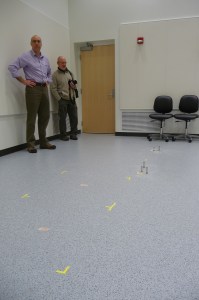
Matt Kramer and Ames Lab science writer Kerry Gibson look over the markings where the aberration-corrected STEM will be installed. (Click on any image for an enlarged view.)
With these instruments, researchers can image materials’ structure at the nanometer scale – a billionth of a meter, or tens of thousands of times smaller than the diameter of a human hair. That lest them distinguish individual atoms or groups of atoms and their arrangement. They can see study the materials’ behavior at different temperatures, under loads and under the influence of electric fields and watch them undergo phase changes, like from liquid to solid, Matt Kramer, director of the Ames Lab’s Materials Science and Engineering Division, noted in a lab release.
With the power of electron microscopy, the researchers can begin designing materials from the atoms up and more quickly focus on compounds that have the greatest potential.
No other building in Iowa has the SIF’s capacity and there are few like it in the Midwest, said Kramer, who showed me around on a December 15 tour. Argonne National Laboratory, another DOE facility near Chicago, has one – but it’s also a much bigger lab.
Oregon-based FEI made the SIF’s microscopes. When I was there, technicians were still tuning the three that were installed and training staff on them. The fourth, the aberration-corrected scanning transmission electron microscope (STEM), was to arrive later in the month. Tape marked its expected location on the floor of its equipment bay.
The aberration-corrected STEM, the FEI Titan, is the microscope most sensitive to vibration and other interference – “so sensitive you don’t want to be in the room” with it, Kramer said. It generates an electron beam finer than the diameter of most atoms. As the beam hits the thin material it’s magnifying, electrons and X-rays scatter. Detectors pick up these scattered particles and rays and translate them into an image. (Here’s an explanation from Purdue University with an assist from ISU.)

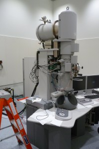
Another look at the transmission electron microscope that was moved to the SIF from the ISU campus. The main tower is where electrons are fired down and focused through apertures and lenses to the sample below, where the eyepieces are located.
As the beam crosses a sample the scattering changes depending on whether it hits a column of atoms or falls between the columns. The degree and pattern of scattering also varies in precise ways depending on which kind of atom is present, as determined by its atomic weight. “Heavy atoms scatter a lot,” Kramer says. “The detector sees it as brighter.”
Underneath the sample, another detector measures how much energy the electron beam lost as it passed through the sample. “Every atom has a characteristic energy absorption level,” so measuring energy lost provides additional information about the material.
Many STEMs have similar detectors. The Titan has four additional X-ray scattering detectors, providing making it more sensitive and faster. “What used to take seconds now can take microseconds” to scan, Kramer said.
ISU helped Ames Lab finance the Titan, guaranteeing university scientists time on the instrument. “One of the things we’re working on is to ensure researchers on campus have just as easy access (to the microscope) as Ames Lab people do,” Kramer says. Faculty in physics, chemistry, materials science and other areas are expected to book time on the Titan.
The next cell to the north holds a transmission electron microscope (TEM) moved from Wilhelm Hall, an Ames Lab building on the ISU campus. It’s not as sensitive to vibration and other interference as the aberration-crrected STEM, Kramer said, but operators could tell when buses passed the building.
When in imaging mode – gathering information about a material’s overall structure – the microscopes’ electron beams are like spotlights, Kramer said. When in scanning mode – characterizing individual atoms – they’re focused, making them more like pencil tips as they move across the sample’s surface.

The focused ion beam (FIB) microscope, which not only produces enlarged images of materials’ structures, but also can sculpt out samples for further study.
But the instrument in the third cell to the north does more than image. The focused ion beam (FIB) microscope also manipulates materials at minute scales.
The FIB pairs a standard scanning electron microscope (SEM) to image materials with a mechanism that generates a beam of gallium ions. The ion beam removes chunks of atoms – at its finest level, on the scale of a few nanometers – allowing researchers to “machine” the material to a precise degree, removing parts only millionths of meters big.
“It lets you sculpt out specific parts of a sample” for analysis, Kramer said. If standard sample preparation is like using an ax, this is like using a scalpel. The FIB even can slice a material like a sausage, allowing researchers to image each and produce a three-dimensional picture of the sample’s structure, similar to how a computed axial tomography (CAT) scanner images “slices” of a person’s body.

Kramer points to areas of a sample that have been “machined” with the FIB’s gallium ion beam. The beam has hollowed out sections of the sample, leaving a thin strip to be removed for further study. The scale indicates the strip is only about 20 millionths of a meter long.
Once researchers machine out a desired section, they can mount it for further study on a different microscope, like the SIF’s fourth device, a field-emission SEM (FE-SEM) in the northernmost instrument bay. As its electron beam moves across the material sample, the FE-SEM provides information about its structure and chemistry. If the material is crystalline (with a repeating atomic structure), the microscope can even determine how the crystals are positioned.
Together, the four instruments are a substantial arsenal for research at Ames Lab and ISU. But there are plans to spread the wealth. Within in a year, Kramer expects off-site scientists – perhaps anywhere in the world – will be able to view microscope images in real time. Eventually, they’ll also be able to control the microscopes remotely, but first technicians must devise a communication system that eliminates all but the tiniest delay between a scientist sending a microscope command and its execution.
The lab has already received inquiries from at least one Midwest university, Kramer said. If all goes well, the SIF could connect materials research across the region, keeping the SIF busy around the clock.